
PCB stands for Printed Circuit Board and it is an electronic component that allows electricity to flow in a circuit. It is used for the interconnection of different electrical components such as resistors, capacitors, diodes and transistors on a single board. These boards are made from high quality materials such as copper and fiberglass to make sure that they are durable enough to withstand high temperatures.
Table of Contents
What is PCB?
A printed circuit board (PCB) is an electronic circuit board manufactured and designed to interconnect electronic components using conductive tracks, pads and other features etched on the printed circuit board substrate. The two main uses of PCBs are as a structural base or substrate for integrated circuits, transistors and other active semiconductor devices, and as a wiring substrate for passive elements such as resistors, capacitors and inductors.
The purpose of this article is to cover all aspects of PCB manufacturing from bare board fabrication to final product assembly.
PCB Manufacturing Process
The PCB manufacturing process is a multi-stage process that begins with the creation of photomasks and ends with final product assembly. In between, there are several steps that must be taken to ensure high quality boards. With the advent of modern PCB manufacturing processes, boards have become more reliable than ever before. This has allowed them to be utilized in a variety of applications that were not previously possible.
The processes become advanced as the time passes. It is important for PCB manufacturers to stay up-to-date with the latest technology in order to produce the best boards possible. Today, the PCB manufacturing process is a multi-stage process that begins with the creation of photomasks and ends with final product assembly. In between, there are several steps that must be taken to ensure high quality boards.
Step 1 – PCB Designing
As a first step, you will need to use your CAD software of choice and create an electronic schematic (also known as a breadboard) for your PCB. This is where all of the components that are going to be placed on the board are assembled together in order to form a functional circuit.
Once this has been done, it’s time to move on to placing them physically on the board itself. This can be done either manually or automatically by using CAM software like EagleCAD, but it’s recommended that you do it manually in order to gain experience with this important stage in producing PCBs.
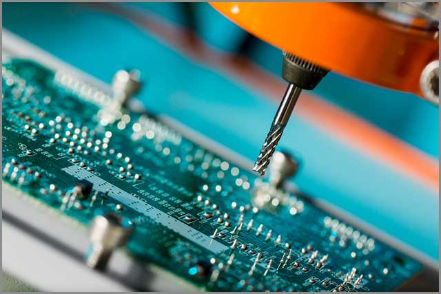
Step 2 – PCB Fabrication and Drilling
The second step in the PCB fabrication process is drilling. This is the process of creating holes in your PCB by using machines. The holes are needed to allow components, connectors and wires to be inserted into the board during assembly.
Step 3 – Through Hole Plating and Silk Screening
The third step in the PCB fabrication process is plating and silk screening. This is the process of adding copper to your PCB by using machines (called “electroplating”) and then applying a protective coating over it to prevent oxidation.
Step 4 – Assembly and Testing
The fourth step in the PCB fabrication process is assembly and testing. This is the process of inserting components into your PCB, connecting them together and then testing your circuit to ensure it functions properly.
Conclusion
After all the above steps, the PCBs are ready to be tested. It is important that every PCB manufacturing company must follow these steps to ensure high-quality boards.


